Novel III-V compound semiconductors and semiconductor nanostructures
Novel III-V compound semiconductors and semiconductor nanostructures for optical and electronical devices
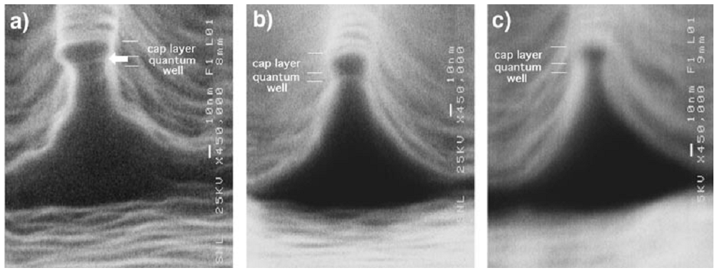
The aim of the research is to provide new high-purity III-V semiconductors by atomic-scale epitaxial and etching techniques. The fields of application concerning the compound semiconductor and nanotechnology based devices include the various LED and laser structures, quantum wire lasers, as well as detectors. The research is supported by various characterisation methods, i.e. Scanning Electron Microscopy (SEM), Energy-Dispersive X-Ray Spectroscopy (EDS), X-Ray Diffractometry (XRD), Auger Electron Spectroscopy (AES), Photoluminescence (PL), Hall Effect Measurement, Secondary Ion Mass Spectroscopy (SIMS).

Tribological simulations – Friction models
Regarding the combustion engines, one of the most critical as well as the most essential current problems is the fuel consumption, which is considered as the primary field of emission reduction. The primary opportunity for an emission reduction can be searched directly at the engine, where the friction losses can be reduced due to the 40-50% responsibility of the piston ring assembly – such as piston, piston rings, and cylinder wall. The reduction of the friction at these components has key importance, because it has a direct influence on wear – as well as have a further effect on the fuel consumption, which determines emission. The aim of the research is to provide models based on the correlations of the friction and wear systems.
RFID and biometrics identification technologies
The aim of the work is to search for new applications of radio-frequency identification systems, as well as improve biometrics identification and their integration for industrial applications.
Contact person: Dr. ZsebőkOttó PhD associate professor Contact information: E-mail: zsebok @ sze.hu, Telephone: +36 96 613-548References:
O. Zsebök: Multifunctional system for sports and leisure complex in HungaryLEGIC News Magazine 1/11 (2011) 12-13.O. Zsebök: Multifunktionales System für Sport- und Freizeitkomplex in UngarnLEGIC News Magazine 1/11 (2011) 12-13. O. Zsebök, J.V. Thordson, L. Ilver and T.G. Andersson:Nanocrystals at MBE-Grown GaN/GaAs(001) InterfacesApplied Surface Science 166 (2000) 317-321. O. Zsebök, J.V. Thordson, R. Gunnarsson, L. Ilver and T.G. Andersson:The effect of the first GaN monolayer on the nitridation damage of MBE-grown GaN on GaAs(001) Journal of Applied Physics 89 (2001) 3662-3666. O. Zsebök, J.V. Thordson, and T.G. Andersson:The formation of nitrogen damage during the growth of GaN on GaAs(001) Japanese Journal of Applied Physics Part 1, 40 (2001) 472-475. O. Zsebök, J.V. Thordson, B. Nilsson and T.G. Andersson:Morphology of InGaAs/GaAs Quantum Wires Prepared by Highly Controlled Deep Etching TechniquesNanotechnology 12 (2001) 32-37.
